Tech Focus: NVIDIA's Kepler Architecture
Digital Foundry on the triumphs and challenges of the new 28nm era
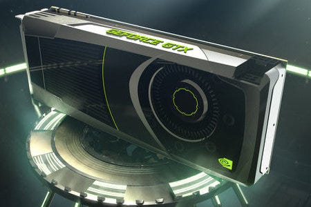

Last week's release of NVIDIA's GeForce GTX 680 graphics card gives us an intriguing look at the thinking of GPU manufacturers as they transition onto the new 28nm fabrication process. The ability to cram more transistors than ever before onto a slice of silicon has been the most significant element in maintaining Moore's Law, and it's also the driving factor in making the next generation consoles a significant, worthwhile technological leap over their predecessors. But NVIDIA's new design targets efficiency as well as power, representing both a triumph and a challenge for what may be difficult times ahead.
"Kepler is a much smaller chip than its Fermi predecessor, sips power in comparison, but still offers 20 to 30 per cent performance boosts. It's the poster child for the new 28nm GPU era."
Let's look at the plus points first, and there are certainly plenty of them. The new NVIDIA architecture, codenamed Kepler, represents a remarkable technological achievement. For a start, let's consider the all-important die-area. The firm's previous flagship card, the GeForce GTX 580, crammed its design onto a piece of silicon measuring 520mm2. The GTX 680 replacement comes in at 295mm2 - a significant reduction in area, especially considering that benchmarks suggest that performance has actually increased by 20 to 30 per cent generally. The efficiency of the design also compares favourably to AMD's new 28nm design: the Radeon HD 7970's GPU occupies a die-area in the region of 325mm2.
Clearly, NVIDIA's focus isn't just to rely on the new fabrication process to cram more transistors into a smaller area, it has gone back to its previous design - the Fermi architecture - redesigning it, achieving superior performance that offers more rendering power per watt consumed. At its recent Editor's Day event in San Francisco, the firm made the bold claim that it is now achieving 2x the performance per watt.
While the specialist PC hardware press have taken that statement to task, the undeniable reality of the achievement remains highly impressive. High-end PC graphics cards had a maximum TDP of 250W - a state of affairs maintained by AMD's Radeon HD 7970. The GTX 680 takes that power draw down to 195W and in the process creates the quietest high-end GPU we've ever used. The achievement also means that the usual six-pin/eight-pin PSU power input required by the card is gone in favour of two six-pin feeds. This means that high-end graphics processing power can now be accommodated by many more PCs and the requirement of a 600W power supply in the chassis is now reduced.
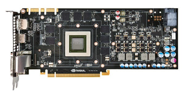
Kepler's efficiency gains are such that there's actually a feeling that NVIDIA is holding back the big guns for future battles. Rumours circulating the hardware press suggest that the GTX 680 was originally designated the GTX 670ti (there's a lot of very convincing evidence to support this) and that its dominance over its top-end AMD rival was such that it was bumped up the product line. This can be seen in elements of the design. High-end GPUs have typically relied in 384-bit memory buses, but the GTX 680 doesn't use that, going with a 256-bit bus instead. Memory throughput isn't so much of an issue with Kepler as remarkably NVIDIA has upped memory clocks to 6GHz, when many thought that exceeding 5.5GHz wouldn't be possible on a mainstream product.
However, the point is that the 384-bit bus remains an option, and rumours point to an even more powerful card with the bus fully restored and possessing 2304 CUDA cores vs. the 1536 in the GTX 580, backed up a 3GB framebuffer (up from 2GB). More interesting though will be the decisions NVIDIA takes to address the mainstream enthusiast sector. The GTX 680 costs £400, but the real volume begins to shift at the £150-£200 price-point. Over the years the company has delivered some remarkably good mid-range GPUs - just one example, the 8800GT, based on the G92 architecture, being so good that it lasted several years (remarkable for a GPU) and was even rebranded into a later generation.
NVIDIA's current mid-range performer, the GTX 560ti has 448 CUDA cores compared to the top-end GTX 580's 512, featuring slower clocks and memory speeds. Applying the same differential to a prospective mid-range version of the GTX 680 suggests an immensely powerful, power efficient card that could easily sit within a console-style chassis such as the Alienware X51. This would make NVIDIA the ideal partner for the hotly rumoured Steam Box concept, but it also means that enthusiast-level GPUs could be added to a vast range of PCs that may have previously had issues running performance-orientated graphics hardware.
In short, for NVIDIA's maiden 28nm outing to so comprehensively outquaff its 40nm predecessor is a superb achievement and finally gives us some idea of what kind of graphical performance we might expect to see in the next-gen consoles, which will also be built with power efficiency in mind. Already we are seeing the GTX 680 being used as a benchmark for next-gen console power - this being the secret Kepler card that Epic used to power its latest version of the Samaritan demo - but we have to remember that the 195W TDP of the card would be equivalent to the entire power budget of a prospective console. However, a GPU even half the size of Kepler, integrated into a fixed hardware architecture could in theory achieve some stunning results.
By way of comparison, the 90nm RSX in the launch PS3 was 240mm2 compared with the 295mm2 of the GTX 680, but in these austere times we shouldn't expect either Microsoft or Sony to invest as heavily in their consoles as they did back in 2005/2006. Efficiency in design is more important than ever.
So if GTX 680 represents the state-of-the-art in terms of power and efficiency with immense room to expand, what are the challenges I mentioned at the beginning of this piece? It's perhaps best summed up this remarkably ExtremeTech story which strongly suggests that NVIDIA feels that the economic benefits of moving to lower fabrication processes are swiftly reaching an end. The provocative headline even suggests that the company feels that the 20nm process is "essentially worthless". This is worrying stuff, with ExtremeTech suggesting that NVIDIA felt compelled to re-architect with efficiency in mind simply because Moore's Law is in danger of no longer being powered by reductions in chip-sizes.
"The suggestion that price per transistor won't fall on the forthcoming 20nm fabrication process puts into question whether the relentless march of GPU power can continue for much longer."
NVIDIA's argument here is very straightforward. In theory we should be looking at a significant reduction in the cost of making a GPU as the area occupied by the chip shrinks dramatically in the transition to a smaller fabrication process. However, certainly at the beginning of this transition, yields on the new process are much lower, increasing costs. NVIDIA is also suggesting that the price of the silicon wafers is increasing too, to the point where the saving on transitioning across is cost-neutral. If the per-transistor cost remains the same, how can Moore's Law be maintained?
This has obvious ramifications for the next-gen consoles. These machines are built at a loss with the sale of software used to claw back costs and eventually make a profit. However, the real profits kick in later on with the release of new console versions - both Xbox 360 and PS3 launched with CPU and GPU on a 90nm process (state-of-the-art for the time, as 28nm is now) but became cheaper to produce over time as the chips were shrunk over time - first to 65nm, then to 45nm. The worrying thing about NVIDIA's warning is that there's a genuine danger that these reductions in cost will no longer be realised - or at the very least, the console makers will have to wait sometime before they happen.
The fabrication plant - TSMC - is the same one used for console CPU/GPU manufacture. The obvious solution to this state of affairs would be to move on to another foundry, but as ExtremeTech points out, if this were any more financially viable, NVIDIA would presumably already have done it, and also cites evidence from AMD that it no longer sees aggressive pursuit of die-shrinks as the primary way forward.
The fact that NVIDIA has gone public at all with the challenges ahead is very telling, but it is suggesting that further collaboration with TSMC along with a fairer share of costs between the companies could make a difference. At the very least, the fact that it has made this argument at all suggests that there is a mutually beneficial way forward that could suit all parties. However, the notion that the effective cost per-transistor in future technology won't be reduced is clearly an obvious concern.
In the meantime, perhaps we should make the most of the here and now. The Kepler architecture remains truly remarkable - a convergence of cooler, smaller technology backed up by superb efficiencies in design. The launch product represents a new state-of-the-art, with enough leeway left in the architecture to produce a wide range of excellent products across a range of price-points - already NVIDIA has demonstrated a Kepler laptop chip capable of running Battlefield 3 at ultra settings with playable frame-rates. For now at least, Moore's Law is safe.